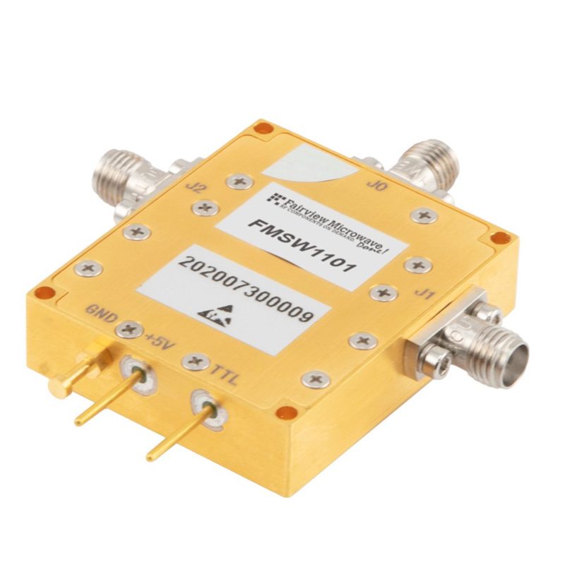
Gallium Nitride (GaN) semiconductors have been a focus of development and innovation in the RF/microwave industry due to the inherent strengths of GaN technology for high power and broadband applications. Compared to Silicon (Si), GaN semiconductors benefit from the material’s wide, direct bandgap (WBG) structure, high electron mobility, and high critical field. This enables GaN devices to be fabricated with comparably higher power in smaller packages, and often leads to other advantages, such as reduced passive component sizes and lower thermal management requirements. Moreover, GaN devices also tend to have relatively high saturation current.

This is also true for GaN-based high-power PIN diode switches, which unlike Si switches, can be designed to reach microwave and even millimeter-wave (mmWave) frequencies. One of the main reasons GaN PIN Diode switch designs can be advantageous over other Class III/V semiconductor technologies, such as gallium arsenide (GaAs) or indium phosphide (InP), is that GaN’s much higher breakdown voltage reduces the need to stack devices to handle higher voltage levels. This is especially important for reflective switch types, as the “off” arm devices under even marginal RF powers of several watts in a 50-ohm system will have to handle RF voltages in the 10s of volts depending on the voltage standing wave ratio (VSWR) of the downstream components. Conversely, “ON” arm switch devices have to handle higher peak currents that at similar levels can exceed an amp. In order for Si, GaAs, or InP devices to handle these types of voltages/currents, they would need to be stacked many times. Using a GaN PIN diode switch technology, reverse biasing of the diode with large voltages ensures the switch is in the “OFF” state and operating at high current levels enables a much lower on-state resistance (RDS_on) while operating in the “ON” state, without the need to excessively stack devices.
Another advantage GaN technology brings to PIN diodes is the much greater broadband performance. One aspect of this is that GaN devices can be made much smaller than other semiconductor technologies designed to handle the same RF power level. Given the overall smaller device size, the related parasitic capacitances are also proportionally smaller, which generally results in better high frequency performance. GaN’s higher voltage operation capability also allows for higher load line impedance, which is desirable for achieving a broadband output match. PIN diode switches, in general, offer good linearity and can reach very high frequencies with good power handling capability.


