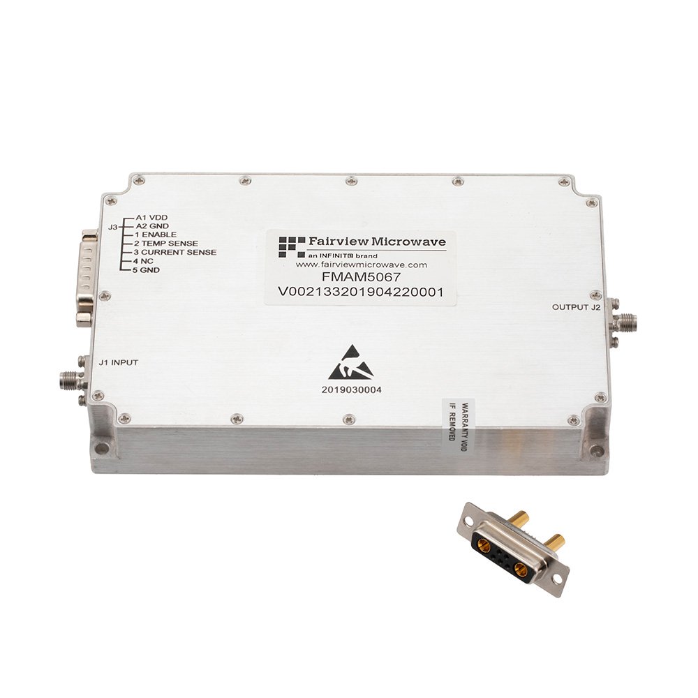
Gallium nitride (GaN) semiconductor technology has been in development for decades. It has also been hyped for many industries as a powerhouse semiconductor technology due to several intrinsic traits of the material. Though not all of the hype has come to fruition, GaN devices such as an RF Power Amplifier or an RF Switch have become widely used in a variety of high power and other applications. The applications where GaN devices are employed continues to grow, as additional efforts to develop the technology, increase the wafer size, and design expertise/tools expand. These developments include working toward complementary metal oxide semiconductor (CMOS) compatible GaN technology, vertical GaN transistors, and GaN devices that operate to hundreds of gigahertz (GHz) and even terahertz (THz).

GaN In Use Today
The main application of current GaN technology is power amplifiers for use in RF/microwave applications. The main reasons that GaN has been able to make such inroads is due to several key device characteristics and GaN-on-insulator technology. These attributes of GaN include a high breakdown voltage (critical electric field), high bandgap voltage, high saturation velocity, and reliable performance even at high temperature extremes (wide operating temperature range). The main type of GaN transistors used are GaN high electron mobility transistors (HEMTs), which exceed indium phosphide (InP) heterobipolar transistors (HBTs), gallium arsenide (GaAs) HBTs, InP HEMTs, and silicon germanium (SiGe) HBTs in breakdown voltage, especially at high frequencies.
Of the two most common variations of GaN-on-insulator technology, GaN-on-SiC (silicon carbide) exceeds GaN-on-Si (Silicon) for power applications as GaN-on-Si tends to exhibit higher epitaxial defects and Si has much lower thermal conductivity than SiC. There are other niche GaN-on-insulator technologies, such as GaN-on-Diamond and GaN-on-Sapphire, but these variants are typically only used in high power military, aerospace, and industrial applications due to high costs and limited availability. Another benefit of GaN HEMTs is that GaN is physically more robust than GaAs or InP, and can generally withstand greater shock and vibration during operation, which makes GaN HEMTs more viable for rugged applications as less design effort and fabrication needs to be expended in ensuring the safety of the device.
Hence, GaN HEMTs have largely been used as power amplifiers, though other uses for GaN amplifiers and transistors are becoming common. For instance, GaN HEMTs are commonly used as broadband amplifiers or a variety of instruments and even active antenna systems (AAS) for wideband millimeter-wave (mmWave) 5G telecommunications. As a single wideband GaN amplifier can handle greater power and a wider bandwidth than other single broadband amplifier solutions, using a GaN broadband amplifier can lead to signal chain benefits in the design where additional splitters/combiners and associated circuitry for combining multiple amplifiers for either higher power or wider bandwidth operation aren’t needed.
GaN low noise amplifiers (LNAs) and switches are also growing in popularity. The same traits that make GaN HEMTs good for high power amplification and broadband applications enable relatively low added noise factor LNAs that are extremely rugged and feature higher survivability than other semiconductors used for LNAs. These same features also allow for more rugged RF/microwave switches that operate over extremely wide bandwidths.
GaN of Tomorrow
Currently, integrating GaN transistors and devices into systems alongside other semiconductor devices and digital electronics is a key focus of a wide range of research. These efforts are focused on bringing GaNs high power and ruggedness in the same packages, or even on the same substrate, as GaAs devices and CMOS digital circuits. Currently, GaN and GaAs multi-chip modules are being made, but future efforts may lead to GaN and GaAs devices on the same substrate. Other efforts include developing CMOS compatible GaN processes, so high density and speed digital circuits can be integrated alongside GaN devices for complete high power and wideband systems-on-a-chip (SoCs).
Another area being explored is developing vertical GaN technology as opposed to today’s lateral GaN HEMTs. It is possible that vertical GaN devices will exhibit higher power density and enable even higher power devices in smaller packages. Vertical devices allow for this as the vertical stack of the transistor element can result in a much higher breakdown voltage than lateral device topologies and vertical devices can often be spaced much closer together for greater transistor density.
The list below highlights some of our bestselling GaN-based products.
FMAM5067 GaN Power Amplifier
FMSW1107 GaN Switch
FAMA1074 GaN Low Noise Amplifier
FM15B5006 GaN Bi-directional Amplifier


